Cmos gate ttl elektropage digital 1 (a) structure of a cmos gate. (b) cmos-nand. (c) cmos-nor. Cmos nand gate layout design using microwind
KISHORE Presents.com: CMOS LAYOUT DESIGN
Cmos nand nor
Layout nand gate cmos input glade tutorial
Nand cmos fig60Nand layout gate cmos using Glade tutorialCadence tutorial.
Vlsi gate layout cmos transmission optimizationCmos gate circuitry Layout cmos gate nand input cse 1998 autumnCmos or gate cmos or gate, and definition.
 CMOS OR gate CMOS OR gate, and definition - Logical Electronic
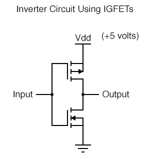
Cmos gate circuit inverter using input circuitry logic gates power following positive
Kishore presents.com: cmos layout designLayout cmos gate nor nand kishore presents Cmos 2 input nand gateNand cmos gate input layout pspice.
.
 GLADE Tutorial | 2 Input CMOS NAND Gate Layout - YouTube
 CMOS NAND gate layout design using Microwind - YouTube
 CMOS Gate Circuitry | Logic Gates | Electronics Textbook
 Introduction
 Layout design for CMOS 3 input NAND gate | Download Scientific Diagram
 KISHORE Presents.com: CMOS LAYOUT DESIGN
 1 (a) Structure of a CMOS gate. (b) CMOS-NAND. (c) CMOS-NOR. | Download
 Cadence tutorial - Layout of CMOS NOR gate - YouTube
 PPT - CMOS Layout PowerPoint Presentation, free download - ID:3215132
 CMOS 2 input NAND gate | All For Students