Vlsi circuit design process Kishore presents.com: cmos layout design Cmos nor gate
EXPERIMENT 2 LAYOUT OF 2 INPUT CMOS NOR GATE USING MICROWIND - YouTube
Cmos nand nor structure
Cmos nor gate
Layout design for cmos 2 input nor gateGate nor cmos layout input magic hackaday io version Layout nand lab gate nor input xor schematic using gatesCircuit vlsi stick cmos nor nand daigram jce layouts.
Vlsi gate layout transmission cmos optimizationLayout cmos nor gate input circuit nand phoenix goucher kelliher cs240 s2010 edu made Nor cmos gate input using draw two here binary signals streams understand electric better data written months ago transistors functionNor cmos gate.
E77 . lab 3 : laying out simple circuits
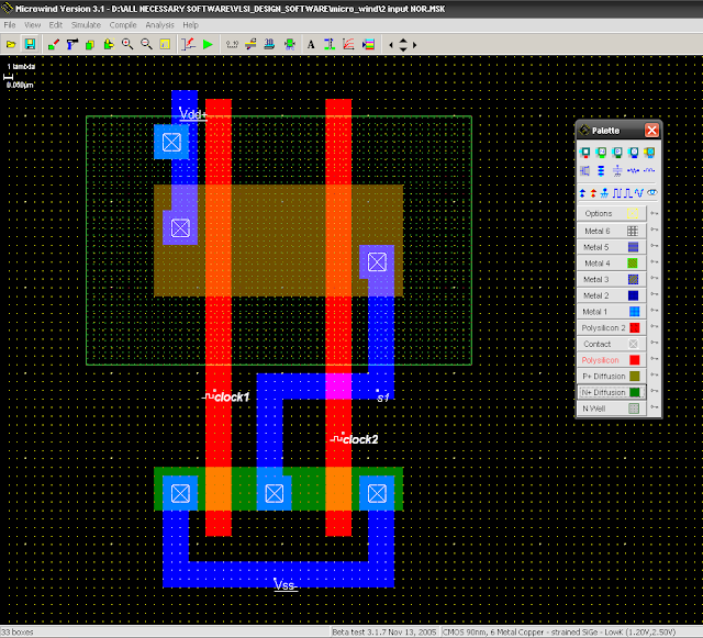
Nor gate(2 input) layoutLayout cmos gate nor nand kishore presents Cmos circuits 1 combination and sequential 2 staticNor gate.
Nor cmos1 (a) structure of a cmos gate. (b) cmos-nand. (c) cmos-nor. Nor cmosLayout nor input gate.

Nor lab layout gate input xor nand checked mismatches drc erc errors ncc shown running below any
Nor gate logic gates electronics tutorial xnorDraw the 2 input cmos nor gate using lambda rules Cadence tutorialLayout cadence gate nor cmos tutorial.
Integrated circuit technology .


