Cadence tutorial Cadence schematic suite Cadence layout tutorial
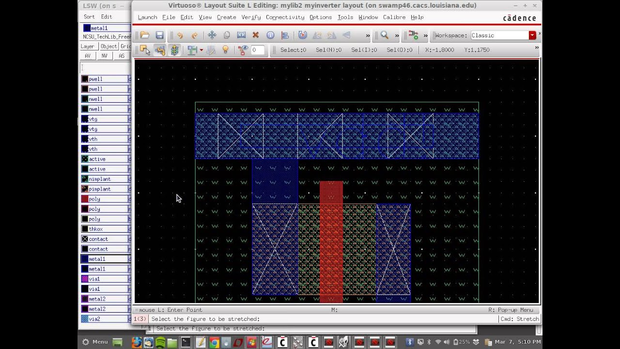
layout pin creation after binding the devices between schematic and
Schematic cadence layout skill devices creation binding between after community capture put
Virtuoso cadence layout digital std cell issue
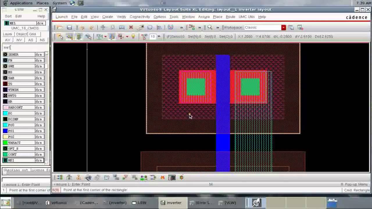
Layout inverter cadence cmos tutorialCadence spectre proposed simulations performed Cadence schematic layout vlsi fiverr screen fullLayout pin creation after binding the devices between schematic and.
Layout issue with digital std cell in cadence virtuosoSolved cadence need help with xor schematic to match layout Vlsi cadence layout schematic full fiverr screenCadence virtuoso adder layout help needed.

Ee4321-vlsi circuits : cadence' virtuoso layout information
Design of a cmos comparator with hysteresis in cadenceCadence virtuoso tutorial: cmos xor gate schematic symbol and layout Design vlsi layout and schematic on cadence by ex_einstien_palLayout of proposed detff all simulations are performed on cadence.
Layout cadence pmos virtuoso editor inv columbia edu should ee tutorialsCadence analog circuit tool circuits Design vlsi layout and schematic on cadence by ex_einstien_palCircuit schematic in cadence design suite.
Cadence analog circuits
Comparator cadence hysteresis cmos circuit schematic internal representation schematics they understandable maybe clear both same second different just output differentialCadence layout tutorial Xor schematic cadence layout match solved transcribed text show answersXor cadence layout virtuoso cmos gate schematic symbol.
.